Can We See Arrangements of Nano Atoms?🤔
Atom Probe Tomography: An CT scan of ATOM
Atom leap is useful in tomography this is something that would leap forward or boost the scientific research in material science area where people can see very small-scale atoms in 3D. Yes !! we are not talking about structure in 3D indeed we are talking about the atom in 3D .
Motivation :
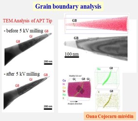
We have a sample where we have clusters inside the material which are of the order of 1NM or 2NM inside that you have atoms if we want to see which atoms are there in the cluster , let us say you have a material and there are some grain boundaries where the elements is getting segregated these region are extremely in small volume and you want to see which element is getting segregated or let say you have CNT and you are embedding some metal to CNT and Diameter of the tube itself is of some Nanometer and you want to see what is getting embed or where is embedded atom seating . This is something what this machine will tell you.
Working :
Basically you make your sample in the form of sharp tip ( like a pen tip ) with extremely thin diameter of the order of 100nm and is kept at very low temperature as low as 50 kelvin.
After this put in machine and apply high voltage and we will see the high field generated . When the field is high then it can pull the atom out of the material/sample . So making the sharp tip is essential to increase the field in order to pull out the atom
So the moment this atom comes out from the tip the time that it takes from tip to a detector which is fixed at the particular distance depends upon the mass of the atom so based on this the time interval is measured from t=0 to moment it his the detector from that the machine detects whether its an Al atom or tungsten atom or Cu atom a per database which is available.
Not only you know the nature of atom but also we know where this atom was setting as the coordinates of atom are retained in the detector layer by layer and we may retrace the sample and build it back again in inside a computer
Application :
1 ) To deign material for this you should know how material behave at small scale and there particular location inside the material
For example : Fast breeders nuclear reactors where the container at which fission material is kept when reaction takes place the temperature are extremely high (750-800o C) now to make a particular steel material to withstand this temperature without getting creeped , some oxide nanoparticle is put inside the grain boundary and pin grain boundary so that creep don’t occur to see and design this properly this tomography play important role .
2 ) Crystal structure of the HEA
HEA are referred as High entopic alloy where more the two elementals are present in equimolar concentration let say more then 20wt% each so in order to recognize it this method is very useful.
Credits www.wikipedia.com
3)Applications in Semiconductor
Semiconductor substances are usually investigated using 3DAPT. Ion implantation may be used to examine the doping percentages at various doping percentages at various parts of the body .
Credits Wikipedia
LIMITATIONS :
1) It is usually useful for elements with higher molecular masses, and hence molecules such as H and He (low molecular weight gasses) are very hard to remove from the chamber and may also get absorbed by the object.
2) The selectable portion can be limited.
3) Materials have a full control over the allowance of the smallest area that can be measured and spectated by us.
Blog Credits : Om Gawande , Srikar Balla - TEAM METAMONDAY
Reference:
1) EEureka Rajya Sabha tvureka Rajya Sabha tv
2) https://nfapt.iitm.ac.in/apt.htmlhttps://nfapt.iitm.ac.in/apt.html
3) http://large.stanford.edu/courses/2014/ph241/rehn2/http://large.stanford.edu/courses/2014/ph241/rehn2/
4) Wikipedia
5) https://www.cameca.com/products/apt/techniquehttps://www.cameca.com/products/apt/technique
NOTE :-
This blog is meant for Educational Purpose only .We do not own any Copyrights related to images and information , all the rights goes to their respective owners . The soul purpose of this blog is to Educate, Inspire, Empower and to create awareness in the viewers. The usage is non-commercial(Not For Profit) and we do not make any money from it.


masta 😐😍
ReplyDelete