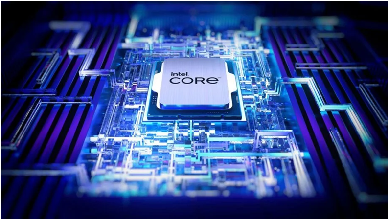
SEMICONDUCTOR CHIP MANUFACTURING
INTRODUCTION
Have
you ever marveled over how far we have come from using flintstones? The human
race's achievements in all technological fields over the last century are far
beyond expectations. The majority of this success is owed to semiconductors.
Semiconductors,
used in ICs, microprocessors, in every electronic device have led to feats in communications,
computing, healthcare, military systems, automobiles, space missions,
artificial intelligence, and every other essential industry.
Are these materials easy to
obtain? How are they actually produced? Let’s have a look.
THE PROCESS
Making semiconductor
devices involve several complicated steps.
1. MINING
The
raw material for most silicon, the most commonly used semiconductor, production
is the mineral quartzite. Raw quartzite is mostly silicon dioxide (SiO2), and
the refining process begins with a reduction reaction to getting rid of the oxygen.
Crushed quartzite is mixed with carbon in the form of coke (coal that has been
heated in the absence of oxygen). We thus obtain pure silicon which is called
an intrinsic semiconductor.
China
is the largest silicon producer in the world, followed right after by Russia,
Brazil, India, and USA. Silicon mines are
of high value due to the vast number of industries semiconductors support.

Source: www.foreignpolicy.com
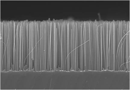
2. WAFER FORMATION
Pure silicon has a monocrystalline structure. Melting in a furnace raw
polysilicon is the first step. The poly is heated to over 1,371°C to purge the
silicon of impurities. The liquified silicon is then spun in one direction,
while a silicon seed, about the size of a pen, is sent down into the molten
silicon and spun in the opposite direction. Spinning in a crucible
bi-directionally speeds the ingot creation with less burden to the system, thus
saving wear and tear on expensive manufacturing equipment. Once cooled, the
silicon crystal seed is pulled from the crucible at a prolonged rate of about
90mm per hour.
The
result is a silicon “ingot”, or wafer in other words.

Source: www.exportersindia.com
3. PHOTORESIST MASKING
A
photomask is an opaque plate with holes or transparencies that allow light to
shine through in a defined pattern, which is applied using lithographic
principles. Lithographic photomasks are typically transparent fused silica
plates covered with a pattern defined with a chromium (Cr) or Fe2O3 metal
absorbing film. Various lithography techniques are used according to the desired
product requirements. Immersion lithography used for ICs, EUV lithography used
for semiconductors dealing with exposure to UV radiation, maskless lithography, and microlithography is some of them.
Manufacturers
subject the wafer to a process of chemical etching that diffuses any areas not
covered by the photoresist film.
The
entire process is conducted in a controlled and clean environment. A single speck of dirt or other foreign
material can ruin the chip, with the potential to cause immense financial
loss.
4. DOPING
Lastly,
the intrinsic material undergoes a crucial step called doping. Trivalent or
pentavalent material is introduced in pure silicon, which increases the conductivity of the material drastically, even at room temperature.
Various
techniques of doping include doping during crystal growth, post-growth doping, and neutron transmutation doping. The impurity material, such as phosphorous,
arsenic or boron, gallium, etc are chosen on the basis of the requirement, thus
converting the dopant material into an n-type or p-type extrinsic semiconductor.
This
process is repeated until the material is covered in patterns, making one layer
of the wafer’s chip. Repeating the process about 100 times with multiple layers
of patterns creates an integrated circuit.
The
wafer is further diced into microchips, giving us the product we usually see.

Source: www.flickr.com
SEMICONDUCTOR MANUFACTURING INDUSTRY
Although silicon is the
industry-giant, materials like germanium, tin oxide, high-power gallium
nitride, Antimonide-based and bismuthide-based materials, Graphene and Pyrite
are widely used.
The top five semiconductor industry leaders, in order of market share, are:
● Intel Corporation ($241.88 billion)
● Samsung Corporation ($221.6 billion)
● NVIDIA Corporation ($152.88 billion)
● Texas Instruments Incorporated ($113.83
billion)
● Broadcom Inc. ($108.13 billion)
Recently, the world has
been facing a chip shortage which is an imminent danger for multiple industries.
The demand for semiconductors has never been greater and is expected to keep
increasing due to emerging technologies such as 5G, AI, and the Internet of
Things (IoT).
The increase in demand has
resulted in an increase in the amount of investments in semiconductor stocks.
INDUSTRY IN INDIA
Taking in mind the
importance of semiconductor manufacturing, the Government of India, through the
Electronics & IT Ministry has come up with new schemes to encourage all
areas of chip-making.
So far, Vedanta, an Indian
multinational mining company, and Taiwanese chipmaker Foxconn have signed an
MoU to set up a ₹1,54,000 crore semiconductor plant in Gujarat. Two other
projects have also been announced — a $3 billion plant in Karnataka by the
International consortium ISMC (a joint venture between Abu Dhabi-based Next
Orbit Ventures and Israel’s Tower Semiconductor) and a $3.5 billion plant in
Tamil Nadu by Singapore’s IGSS Ventures. The modified scheme also emphasizes
the production of the 45nm chip, which is fairly less time-consuming and
economical in terms of production. These chips have high demand, driven
primarily by automotive, power, and telecom applications.
Semiconductor manufacturing
is thus a promising, flourishing, and rapidly growing industry. It demands
attention from investors around the world and also ensures exponential in AI,
5G, IoT, and other influential industries.
CREDITS:
Aarya Kulkarni (112107001) SY EnTC
RESOURCES:
● https://en.wikipedia.org/wiki/Doping_(semiconductor)
NOTE:
This blog is meant for educational
purposes only. We do not own any Copyrights related to images and information,
all the rights go to their respective owners. The sole purpose of this blog is
to Educate, Inspire, Empower, and create awareness in the viewers. The usage is
non-commercial(Not For Profit) and we do not make any money from it.
Write your feedback here:
https://forms.gle/C3ybXMPPUaJBgP618
FOLLOW US ON:
INSTAGRAM :
https://bit.ly/coep_blogs_insta
LINKEDIN:
https://bit.ly/coep_blogs_linkedIn
YOUTUBE:-

A well-written and informative blog post that highlights the promising Future Of Semiconductor Industry In India. The author's ability to convey complex information in a simple and engaging manner is commendable
ReplyDelete